Energy filter for ion implantation systems
For the production of electronic components, such as ICs, power transistors or diodes, the properties of the semiconductor are defined by introducing dopants. Silicon is doped by irradiating it with high-energy ions. The design of ion implanters means that the ions hit the material to be implanted with a fixed kinetic energy. As a result, the ions come to rest in the material at a defined depth and with a known, relatively narrow distribution. In many cases, however, it is desirable to have a continuum of energies available in an ion beam rather than just ions of one energy and thus to be able to generate doping in a wider depth window. This problem is to be solved in the "Energy filter for ion implantation systems" project. The idea of the energy filter is outlined in Figure 1.
The filter [1] consists of a thin membrane (0.5 - 1.0 μm thick) on which the actual triangular silicon filter structures are arranged by means of lithography and anisotropic silicon etching. Accelerated ions hit the filter element and - depending on whether they have to travel a long or short distance in the filter material - will suffer a large or small loss of energy. This results in a continuous energy distribution of the ions in a window defined by the filter geometry and thus the distribution of the ions over a larger depth range. The depth profile (concentration over depth) can be adjusted by the shape of the filter. A closer look at the situation in Fig. 1 shows that the arrangement maps the three-dimensional serrated structure of the filter into the substrate, i.e. the locations of minimum and maximum implantation depth do not lie on top of each other. This is undesirable.
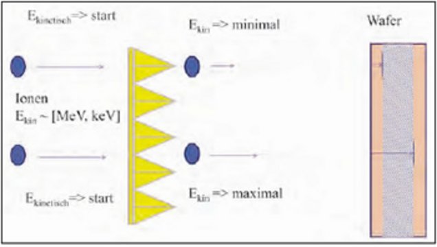
The idea of the energy filter is outlined in Figure 1. The filter [1] consists of a thin membrane (0.5 - 1.0 μm thick) on which the actual triangular silicon filter structures are arranged by means of lithography and anisotropic silicon etching. Accelerated ions hit the filter element and - depending on whether they have to travel a long or short distance in the filter material - will suffer a large or small loss of energy. This results in a continuous energy distribution of the ions in a window defined by the filter geometry and thus the distribution of the ions over a larger depth range. The depth profile (concentration over depth) can be adjusted by the shape of the filter. A closer look at the situation in Figure 1 shows that the arrangement maps the three-dimensional serrated structure of the filter into the substrate, i.e. the locations of minimum and maximum implantation depth do not lie on top of each other. This is undesirable.
The results to date
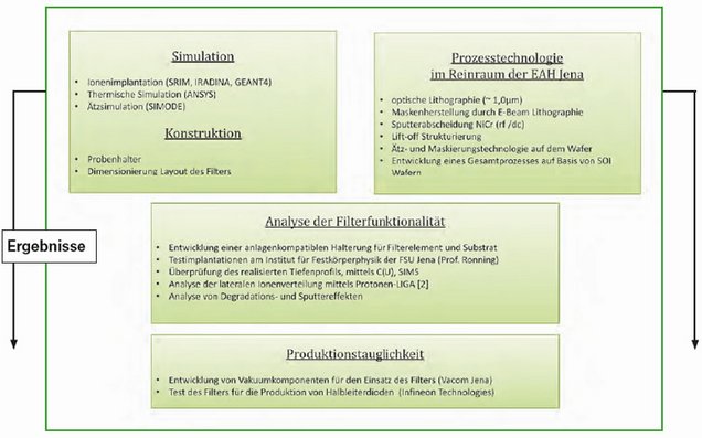
The main work packages are shown in Figure 3. Following this project structure, important results were achieved last year.
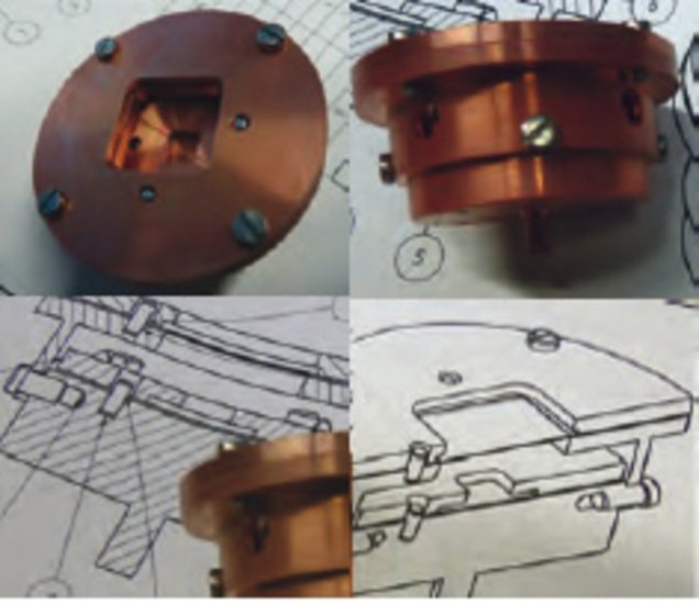
The first sample and filter holder for implantation tests was produced, see Figure 2, and is a prerequisite for being able to carry out tests on the Tandetron JULIA at the FSU Jena. The primary aim of the previous simulations was to realise a suitable dimensioning of the filter element and to understand the problem of the lateral distribution of the ions.
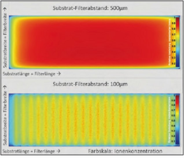
At the bottom, the red vertical stripes (concentration maxima) show that the structure of the filter is transferred at a filter distance of 100 µm. The top shows that the structure is no longer visible at a distance of 500 µm.
It can be seen that the backup solution, namely a mechanical oscillating movement of the filter to achieve a homogeneous lateral distribution of the ions, is not necessary if filter sample distances in the millimetre range are realised (see Figure 4).
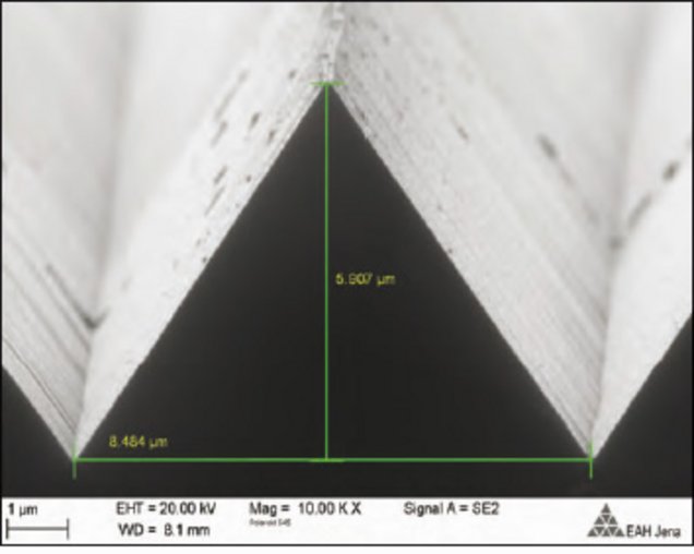
Figure 5 shows a result of microtechnical silicon processing in the clean room. Further work will focus on optimising the overall process sequence for manufacturing the filter and carrying out initial functionality tests on the ion implanter. Furthermore, the application possibilities for use in the semiconductor industry and medicine (tumour heavy ion therapy) are being evaluated.
Literature
[1] M. Rüb: German Patent Application No. 102011075350.8
[2] F. Schrempel, W. Witthuhn: Nuclear instruments and methods in physics research B, Vol.132, 1997, pp.430 - 438.
