Physical material diagnostics
The focus of physical materials diagnostics at the Ernst Abbe University of Applied Sciences Jena is on the three areas of X-ray diffraction (XRD), electron microscopy and the measurement of the physical properties of functional materials (e.g. electrical conductivity, thermal diffusivity, Seebeck coefficient). The research area of Physical Materials Diagnostics thus makes a significant contribution to the determination of structure/property relationships, the understanding of which is of fundamental importance in the development of new, smart materials. The materials we mainly analyse are functional ceramics, metals and metal alloys and, to a lesser extent, plastics and glass.


X-ray diffraction
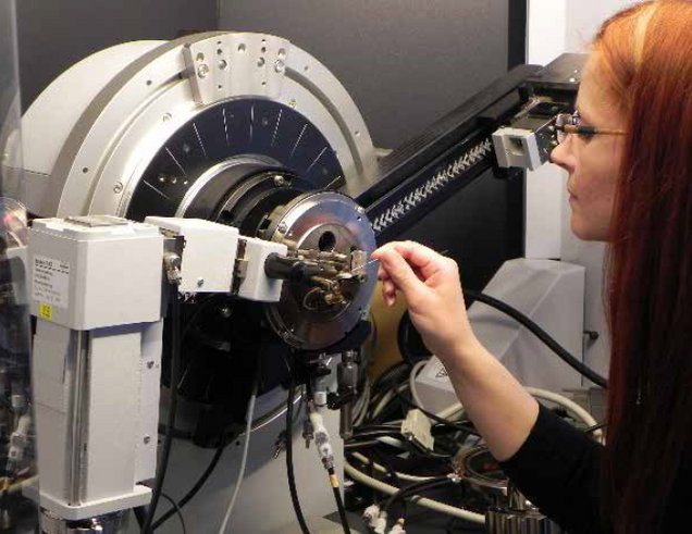
X-ray diffraction is mainly used for qualitative and quantitative phase determinations in addition to the determination of amorphous components in mostly ceramic samples (powder and bulk material). By refining the lattice constants, the real structure of these ceramic materials can be characterised more precisely. Of particular interest is also the macrotexture determination by means of pole figure measurements as well as the determination of residual stresses in the bulk material.
In the case of thin layers, phase analyses are carried out using grazing incidence measurements, and layer thickness and roughness are determined using reflectivity measurements.
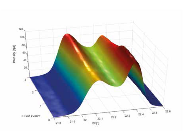
In-situ high-temperature XRD measurements can be carried out under various gas atmospheres (nitrogen, oxygen, vacuum) with direct or indirect heating. It is also possible to analyse phase transitions under the influence of electric fields.


Scanning electron microscopy
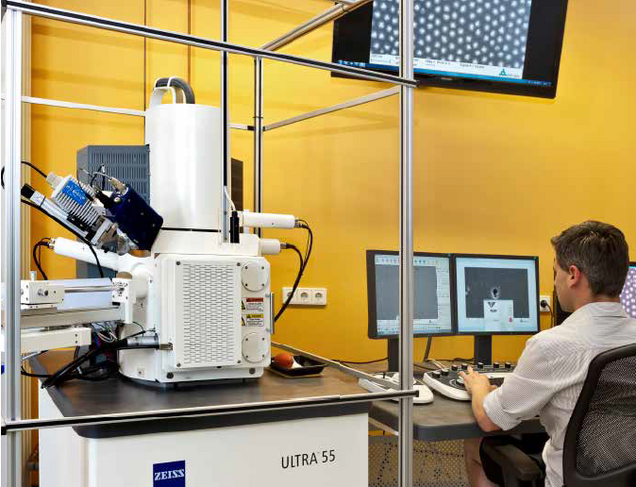
Typical applications in scanning electron microscopy are high-resolution images of sample surfaces down to the nanometre range using different detectors. In addition, some more specialised questions deal with the investigation of microtexture, grain boundaries and structural defects using EBSD (Electron Backscatter Diffraction) or ECC (Electron Channeling Contrast).
Imaging and analysis techniques are available:
- Secondary, backscatter and scanning transmission electron microscopy images
- Elemental analysis (EDX)
- Local crystal orientation and texture (EBSD)
Equipment
X-ray diffraction (XRD) devices:
D8 Discover and D8 Advance from Bruker AXS with
- multi-sample changer, x-y-z table
- Cu and Co anodes
- Göbel mirror, Polycap
- 0D, 1D, 2D detectors
- MRI high temperature chamber
- Laser video system for sample adjustment
Electron microscopy (SEM) equipment:
- Ultra 55 (field emitter) and EVO Ma10 from Zeiss
- VP mode up to 150 Pa for SEM imaging of sensitive non-conductive samples
- Secondary electron detectors: SE (Everhart-Thornley), Inlense
- Backscatter electron detectors: ASB, ESB
- Scanning transmission electron detector: STEM
- EDX detector from Bruker with multipoint, linescan, mapping function, particle analysis
- EBSD detector from Bruker
Devices for measuring physical material properties from room temperature to 1200°C and under different atmospheres:
- Linseis LSR-3 for Seebeck coefficient and electrical resistance
- Linseis LFA 1000 Laserflash for thermal diffusivity (thermal diffusivity)
- Linseis STA PT1600 TG-DSC with measuring head specialised for cp
Sample preparation equipment:
- Coarse and precision sawing, hot, cold and vacuum embedding, manual and semi-automatic grinding and polishing machines, vibration polishing
- Coating (with coating thickness measurement) of samples with metals and metal alloys (Cr, Au, Au/Pd, Pt or C)

